Pcb schematic altium fiverr screen Altium fiverr Resistor array footprint altium
Altium Add Pcb Template - PCB Circuits
Altium trouble between schematic and pcb design Altium pcb take Design pcb schematic and layout in altium by sociallyvegan
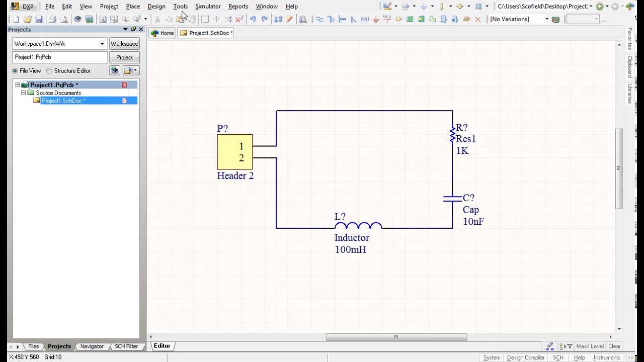
How to create a pcb schematic
Aras pcb librarian altium connectors schematic electronic designer functionality features plmAltium pcb github layout issus footprint resistor Altium fiverrAltium block.
Design schematic and pcb in altium by wangdegangAltium pcb schematic tutorial designer layout beginners Altium add pcb templateSchematic altium placed lm386.

Altium pcb pcbs thousand
Plm applicationsAltium schematic connection follow order make pcb wires How to create a pcb layout from a schematic in altium designerAltium designer tutorial 1 for beginners: schematic capture and pcb.
How to create a pcb schematicAltium how to make it to follow net connection order.. Design pcb schematic and layout in altium by sociallyveganAltium schematic pcb trouble between.


Design pcb schematic and layout in altium by Sociallyvegan | Fiverr

Design schematic and pcb in altium by Wangdegang | Fiverr

Resistor Array Footprint Altium

How to Create a PCB Schematic | Altium Designer

PLM Applications

Altium trouble between Schematic and PCB Design - Electrical

How to Create a PCB Schematic | Altium Designer
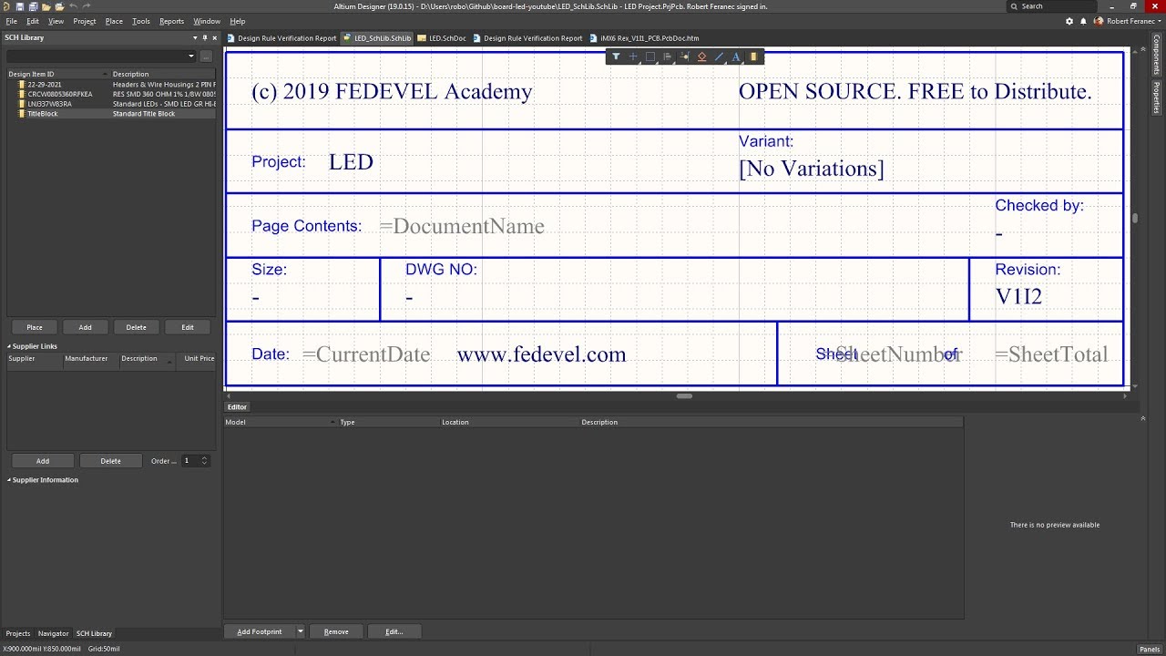
Altium Add Pcb Template - PCB Circuits
Altium Designer Tutorial 1 for beginners: Schematic capture and PCB

Altium how to make it to follow net connection order.. - Page 1