Schematic diagrams compared other wiring layouts engineering electrical Schematic ourpcb wires connect must guidelines diagram good point four Pcb reverse engineering, expert pcb copy engineering service
PCB Layout and Trace Widths for Buck Converter - Electrical Engineering
Pcb design Printed circuit board design, diagram, assembly Pcb buck layout converter trace widths schematic stack
Wiring schematic
Schematic and pcb designDiagram schematic basics circuits lying mastering component 6 updating the pcb from the schematicPcb schematic – arxterra.
Pcb circuit board layout diagram printed drawing assembly electronics prototype electronic components service boards schematics two softwareSmps pcb pfc layout 4kva schematic fullbridge pdf circuit electronic ni tested Smps fullbridge pfc schematic + pcb layout pdfHow to create a pcb layout from a pcb schematic in altium designer.

Pcb converting schematic easyeda layout diagram tutorial using component arrange step
Pcb schematic komatsu startsSchematic pcb altium designed Pcb qualityinspection schematic march simulationPcb layout electronic circuit schematic diagram engineering generator envelope adsr voltage controlled services reverse vc 7b datasheet development.
Mastering the art of pcb design basicsPcb layout and trace widths for buck converter Pcb layout schematicsFree pcb schematic entry & layout software beat eagle for some features.

Guidelines for a good schematic diagram
How to design a pcb layoutTeach you how to draw a simple pcb schematic in seven steps – so good Schematic measurementPcb layout using easyeda|converting schematic diagram to pcb design.
Pcb altium layoutPcb schematic layout software Online schematic pcbHow to design a pcb layout.

Pcb layout needs improvement
Pcb layout schematic improvement needs usb stack .
.


March 2015 - QualityInspection.org
6 Updating the PCB from the schematic - YouTube

SMPS FULLBRIDGE PFC Schematic + PCB Layout PDF - Electronic Circuit

PCB layout needs improvement - Electrical Engineering Stack Exchange

Guidelines for a good schematic diagram - PCB Assembly,PCB

Printed Circuit Board Design, Diagram, Assembly - Steps, Tutorial

Mastering the Art of PCB Design Basics | Sierra Circuits

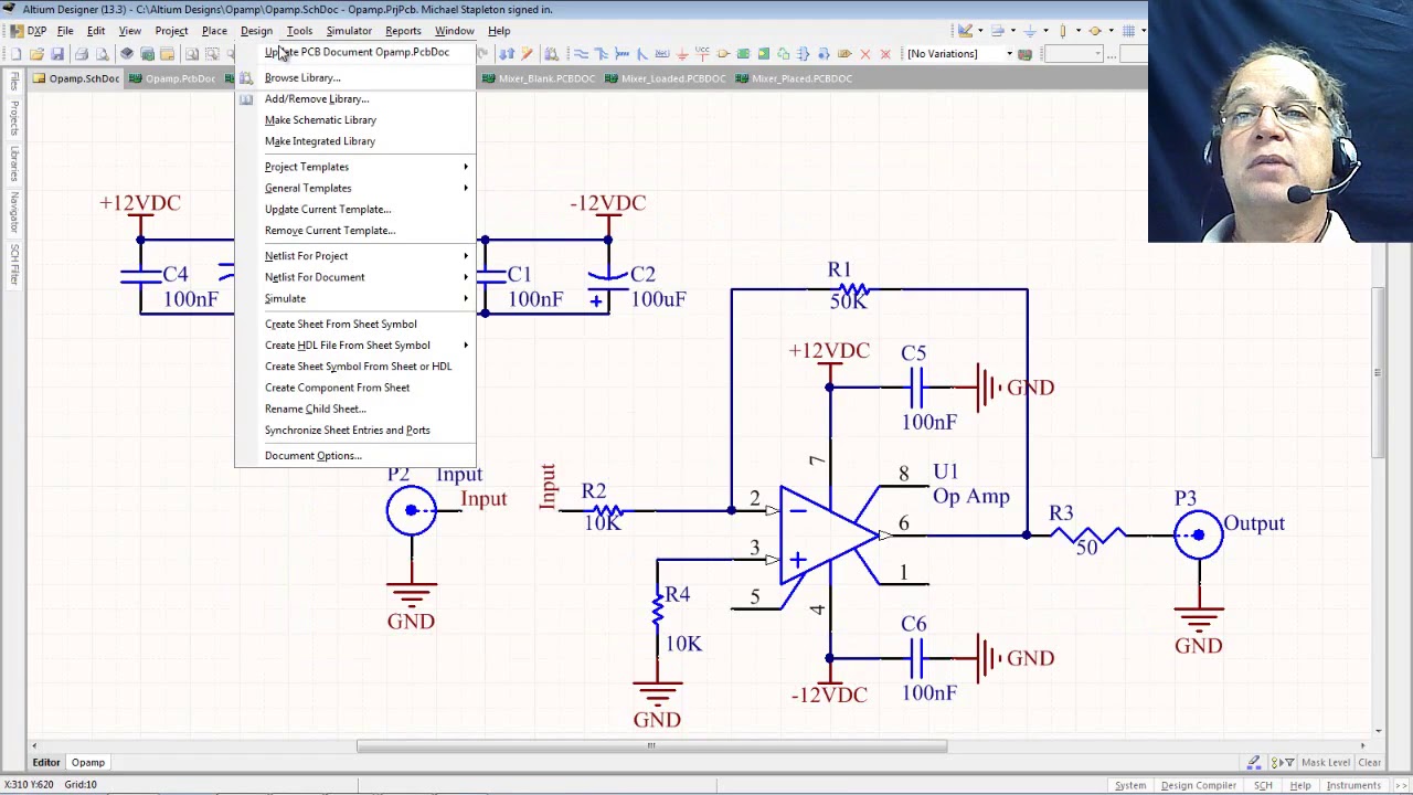
How to Create a PCB Layout from a PCB Schematic in Altium Designer